- 您现在的位置:买卖IC网 > Sheet目录1999 > ICS87973DYI-147LF (IDT, Integrated Device Technology Inc)IC CLK MULT/ZD BUFFER 52TQFP
ICS87973I-147
LOW SKEW, 1-TO-12, LVCMOS/LVTTL CLOCK MULTIPLIER/ZERO DELAY BUFFER
IDT / ICS LVCMOS CLOCK MULTIPLIER/ZERO DELAY BUFFER
10
ICS87973DYI-147 REV. A DECEMBER 9, 2008
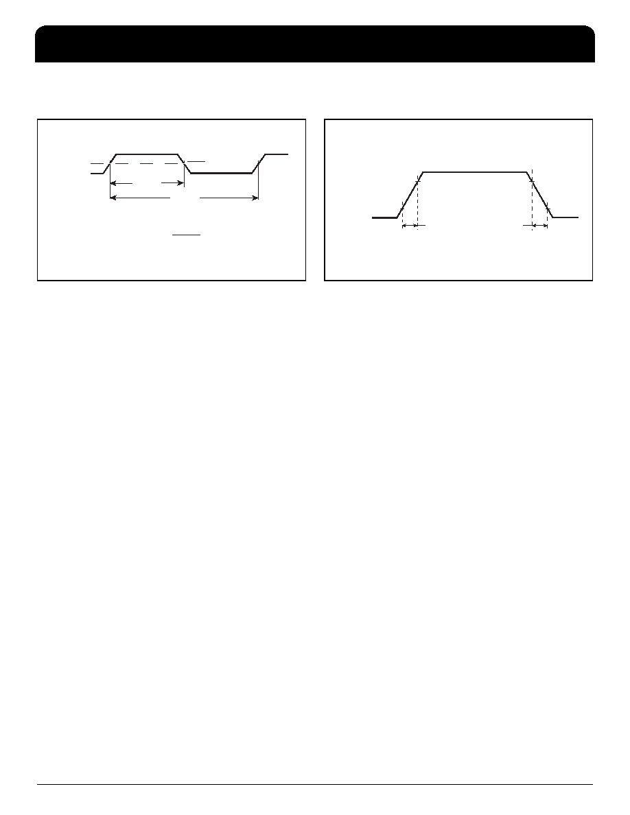
Parameter Measurement Information, continued
Output Duty Cycle/Pulse Width Period
Output Rise/Fall Time
Application Information
Recommendations for Unused Input and Output Pins
Inputs:
CLK/nCLK Inputs
For applications not requiring the use of the differential input, both
CLK and nCLK can be left floating. Though not required, but for
additional protection, a 1k
resistor can be tied from CLK to
ground.
CLK Inputs
For applications not requiring the use of the clock input, it can be
left floating. Though not required, but for additional protection, a
1k
resistor can be tied from the CLK to ground.
LVCMOS Control Pins
All control pins have internal pull-ups; additional resistance is not
required but can be added for additional protection. A 1k
resistor
can be used.
Outputs:
LVCMOS Outputs
All unused LVCMOS output can be left floating. There should be no
trace attached.
t
PERIOD
t
PW
t
PERIOD
odc =
V
DDO
2
x 100%
t
PW
QA[0:3],
QB[0:3],
QC[0:3],
QSYNC,
QFB
0.8V
2V
0.8V
tR
t F
QA[0:3],
QB[0:3],
QC[0:3],
QSYNC,
QFB
发布紧急采购,3分钟左右您将得到回复。
相关PDF资料
ICS87973DYILFT
IC CLK MULT/ZD BUFFER 52-LQFP
ICS87974CYILF
IC CLK GEN LVCMOS/LVTTL 52-LQFP
ICS894D115AGI-04LF
IC CLK/DATA RECOVERY 20-TSSOP
ICS894D115BGI-01LF
IC CLK/DATA RECOVERY 20-TSSOP
ICS9112AM-17LF
IC BUFFER HI PERFORMANCE 16-SOIC
ICS91305AMILF
IC CLOCK DRIVER LO JITTER 8-SOIC
ICS91305AMLF
IC CLOCK DRIVER LO JITTER 8-SOIC
ICS91309AGILF
IC CLK BUFFER ZD PLL 16TSSOP
相关代理商/技术参数
ICS87973DYI-147LFT
功能描述:IC CLK MULT/ZD BUFFER 52TQFP RoHS:是 类别:集成电路 (IC) >> 时钟/计时 - 时钟发生器,PLL,频率合成器 系列:HiPerClockS™ 标准包装:1,000 系列:- 类型:时钟/频率合成器,扇出分配 PLL:- 输入:- 输出:- 电路数:- 比率 - 输入:输出:- 差分 - 输入:输出:- 频率 - 最大:- 除法器/乘法器:- 电源电压:- 工作温度:- 安装类型:表面贴装 封装/外壳:56-VFQFN 裸露焊盘 供应商设备封装:56-VFQFP-EP(8x8) 包装:带卷 (TR) 其它名称:844S012AKI-01LFT
ICS87973DYILF
功能描述:IC CLK MULT/ZD BUFFER 52-LQFP RoHS:是 类别:集成电路 (IC) >> 时钟/计时 - 时钟发生器,PLL,频率合成器 系列:HiPerClockS™ 标准包装:2,000 系列:- 类型:PLL 频率合成器 PLL:是 输入:晶体 输出:时钟 电路数:1 比率 - 输入:输出:1:1 差分 - 输入:输出:无/无 频率 - 最大:1GHz 除法器/乘法器:是/无 电源电压:4.5 V ~ 5.5 V 工作温度:-20°C ~ 85°C 安装类型:表面贴装 封装/外壳:16-LSSOP(0.175",4.40mm 宽) 供应商设备封装:16-SSOP 包装:带卷 (TR) 其它名称:NJW1504V-TE1-NDNJW1504V-TE1TR
ICS87973DYILFT
功能描述:IC CLK MULT/ZD BUFFER 52-LQFP RoHS:是 类别:集成电路 (IC) >> 时钟/计时 - 时钟发生器,PLL,频率合成器 系列:HiPerClockS™ 标准包装:1,000 系列:- 类型:时钟/频率合成器,扇出分配 PLL:- 输入:- 输出:- 电路数:- 比率 - 输入:输出:- 差分 - 输入:输出:- 频率 - 最大:- 除法器/乘法器:- 电源电压:- 工作温度:- 安装类型:表面贴装 封装/外壳:56-VFQFN 裸露焊盘 供应商设备封装:56-VFQFP-EP(8x8) 包装:带卷 (TR) 其它名称:844S012AKI-01LFT
ICS87974CYILF
功能描述:IC CLK GEN LVCMOS/LVTTL 52-LQFP RoHS:是 类别:集成电路 (IC) >> 时钟/计时 - 时钟发生器,PLL,频率合成器 系列:HiPerClockS™ 标准包装:1,000 系列:- 类型:时钟/频率合成器,扇出分配 PLL:- 输入:- 输出:- 电路数:- 比率 - 输入:输出:- 差分 - 输入:输出:- 频率 - 最大:- 除法器/乘法器:- 电源电压:- 工作温度:- 安装类型:表面贴装 封装/外壳:56-VFQFN 裸露焊盘 供应商设备封装:56-VFQFP-EP(8x8) 包装:带卷 (TR) 其它名称:844S012AKI-01LFT
ICS87974CYILFT
功能描述:IC CLOCK GEN 1-15 PLL 52-LQFP RoHS:是 类别:集成电路 (IC) >> 时钟/计时 - 时钟发生器,PLL,频率合成器 系列:HiPerClockS™ 标准包装:1,000 系列:- 类型:时钟/频率合成器,扇出分配 PLL:- 输入:- 输出:- 电路数:- 比率 - 输入:输出:- 差分 - 输入:输出:- 频率 - 最大:- 除法器/乘法器:- 电源电压:- 工作温度:- 安装类型:表面贴装 封装/外壳:56-VFQFN 裸露焊盘 供应商设备封装:56-VFQFP-EP(8x8) 包装:带卷 (TR) 其它名称:844S012AKI-01LFT
ICS879893AYILF
功能描述:IC CLK GEN LVCMOS/LVTTL 48-LQFP RoHS:是 类别:集成电路 (IC) >> 时钟/计时 - 时钟发生器,PLL,频率合成器 系列:HiPerClockS™ 标准包装:1,000 系列:- 类型:时钟/频率合成器,扇出分配 PLL:- 输入:- 输出:- 电路数:- 比率 - 输入:输出:- 差分 - 输入:输出:- 频率 - 最大:- 除法器/乘法器:- 电源电压:- 工作温度:- 安装类型:表面贴装 封装/外壳:56-VFQFN 裸露焊盘 供应商设备封装:56-VFQFP-EP(8x8) 包装:带卷 (TR) 其它名称:844S012AKI-01LFT
ICS879893AYILFT
功能描述:IC CLK GEN LVCMOS/LVTTL 48-LQFP RoHS:是 类别:集成电路 (IC) >> 时钟/计时 - 时钟发生器,PLL,频率合成器 系列:HiPerClockS™ 标准包装:1,000 系列:- 类型:时钟/频率合成器,扇出分配 PLL:- 输入:- 输出:- 电路数:- 比率 - 输入:输出:- 差分 - 输入:输出:- 频率 - 最大:- 除法器/乘法器:- 电源电压:- 工作温度:- 安装类型:表面贴装 封装/外壳:56-VFQFN 裸露焊盘 供应商设备封装:56-VFQFP-EP(8x8) 包装:带卷 (TR) 其它名称:844S012AKI-01LFT
ICS87993AYILF
功能描述:IC PLL CLK DRIVER 1-5 32-LQFP RoHS:是 类别:集成电路 (IC) >> 时钟/计时 - 时钟发生器,PLL,频率合成器 系列:HiPerClockS™ 标准包装:1,000 系列:- 类型:时钟/频率合成器,扇出分配 PLL:- 输入:- 输出:- 电路数:- 比率 - 输入:输出:- 差分 - 输入:输出:- 频率 - 最大:- 除法器/乘法器:- 电源电压:- 工作温度:- 安装类型:表面贴装 封装/外壳:56-VFQFN 裸露焊盘 供应商设备封装:56-VFQFP-EP(8x8) 包装:带卷 (TR) 其它名称:844S012AKI-01LFT